Complete Guide to PN Junction Diode [Updated] Characteristics

How A Pn Junction Diode Works Dr Bakst
The PIN photodiode was invented by Jun-Ichi Nishizawa and his colleagues in 1950. It is a semiconductor device. Operation A PIN diode operates under what is known as high-level injection. In other words, the intrinsic "i" region is flooded with charge carriers from the "p" and "n" regions.
pn Junction Diode Definition, Formation, Characteristics, Applications
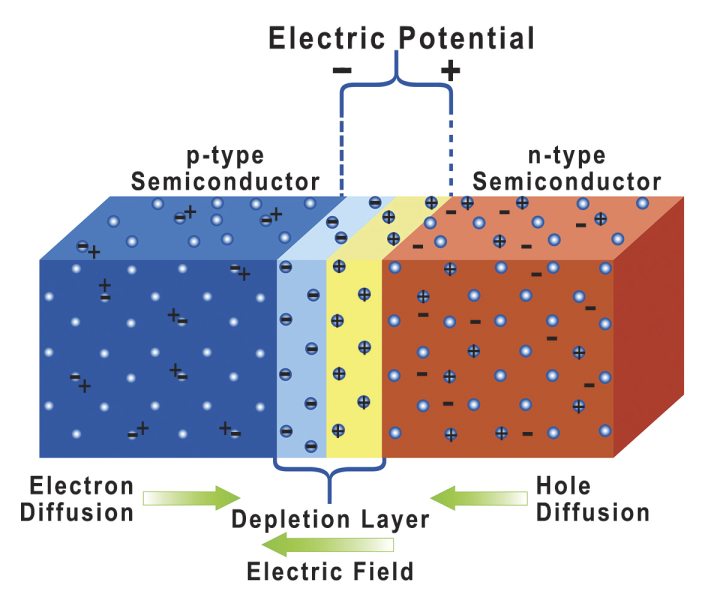
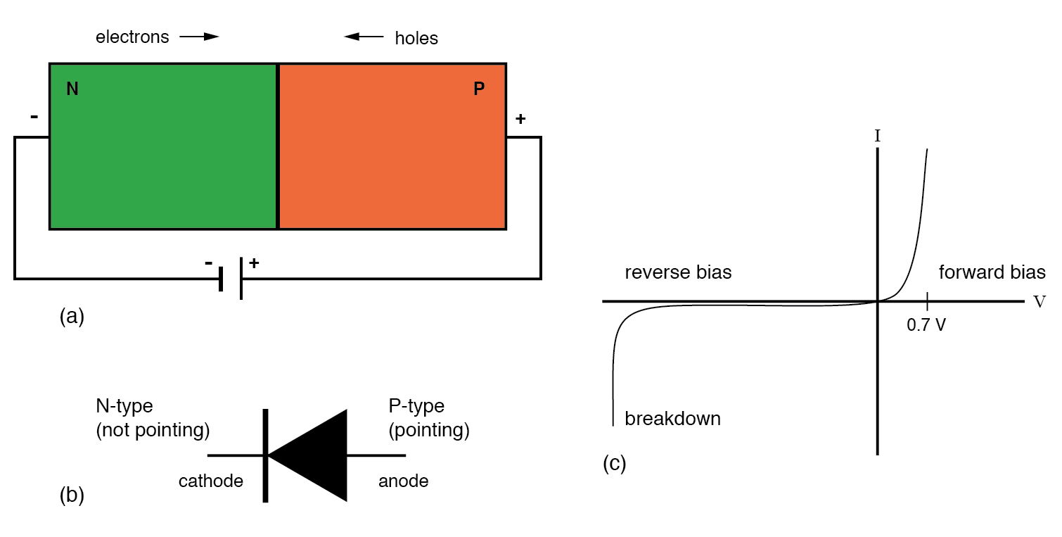
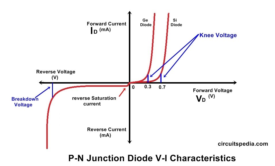
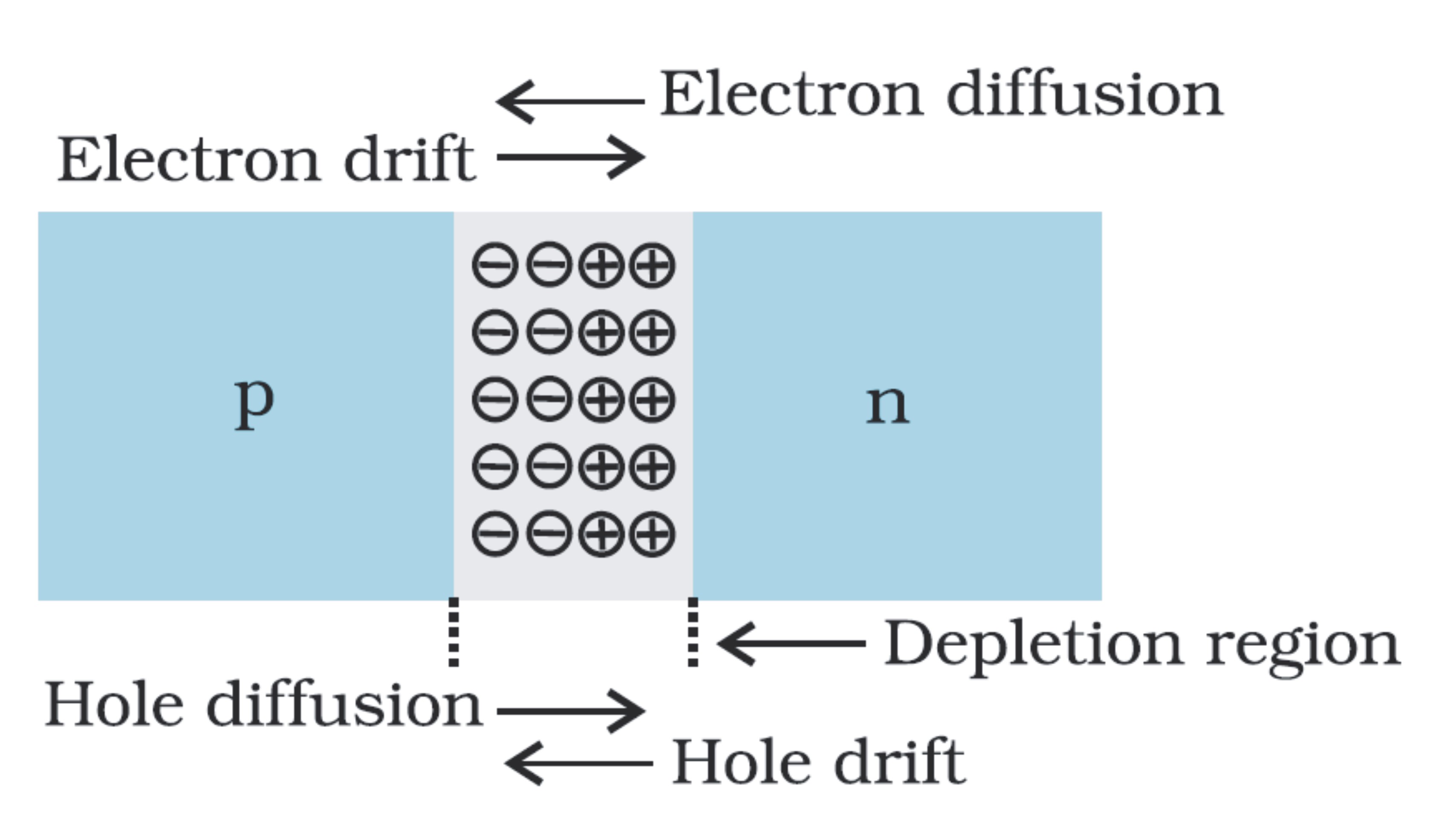
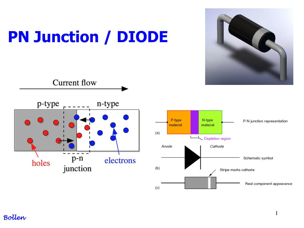
A p-n junction. The circuit symbol is shown: the triangle corresponds to the p side. A p-n junction is a boundary or interface between two types of semiconductor materials, p-type and n-type, inside a single crystal of semiconductor. The "p" (positive) side contains an excess of holes, while the "n" (negative) side contains an excess of electrons in the outer shells of the electrically.

☑ Pn Junction Diode Wikipedia
PIN diode Structures J.Y. Wah, C. J. Hepburn Overview A p-i-n diode is a p-n junction with a doping profile tailored so that an intrinsic layer, the 'i region,' is sandwiched between a p layer and an n layer. In practice, however, an idealized i region is.
Complete Guide to PN Junction Diode [Updated] Characteristics
A PIN diode is a type of diode having undoped intrinsic semiconductor region placed between two regions called p-type semiconductor and the n-type semiconductor region. These two regions are primely heavily doped as they find applications for ohmic contacts. Characteristics of Pin Diode

Simplified energy band diagram of a pin junction. Download Scientific Diagram
The PIN diode is a one type of photo detector, used to convert optical signal into an electrical signal. The PIN diode comprises of three regions, namely P-region, I-region and N-region.

Pn Junction Diode Working Principle Animation Ppt
January 18, 2021 by Electricalvoice Pin diode is a type of diode that has p-type and n-type semiconductor material sandwiching an intrinsic layer. The intrinsic layer is a layer of undoped semiconductor material. This is the structural difference between a normal PN junction diode and a PIN junction diode.

PN Junction Diode and VI Characteristics Explained YouTube
The PIN diode is a type of photodetector used for converting the light energy into the electrical energy. The intrinsic layer between the P and N-type regions increases the distance between them. The width of the region is inversely proportional to their capacitance.
PN Junction Diode Formation, Symbol, Biasing, VI Characteristics, Application » ElectroDuino
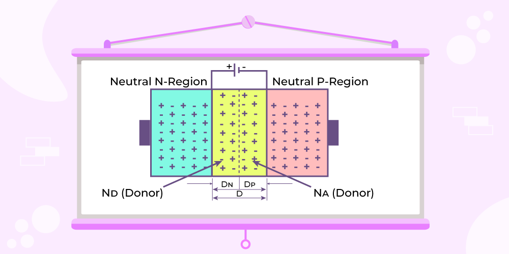
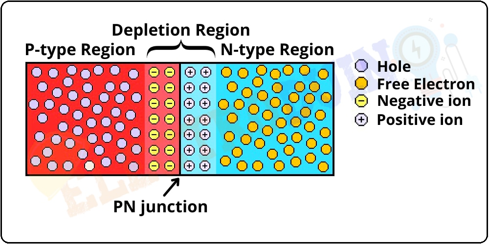
A PN-junction diode is formed when a p-type semiconductor is fused to an n-type semiconductor creating a potential barrier voltage across the diode junction The PN junction diode consists of a p-region and n-region separated by a depletion region where charge is stored.

PN junction diodes (LIV) M Dash Foundation C Cube Learning
Definition: A PIN diode is an advancement of normal PN junction diode. It is a 3-layer device in which an intrinsic layer i.e., undoped semiconductor is sandwiched between P and N regions. Thus, making it a PIN diode. The presence of intrinsic region exhibits high resistance property.
Diode Physics
A PIN diode is a diode with a large and undoped intrinsic semiconductor region which is wedged between a p-type and an n-type semiconductor region. Since they are used for ohmic connections, the p-type and n-type regions are usually highly doped. In comparison to a standard p-n diode, this diode has a large intrinsic field.
The PN Junction Solidstate Device Theory Electronics Textbook
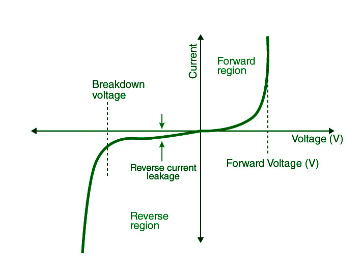
The pn Junction Diode -- Uses: Rectification, parts of transistors, light-emitting diodes and lasers, solar cells, electrically variable capacitor (varactor diode), voltage reference (zener diode) Depletion region & junction capacitance I-V characteristic Circuit applications and analysis Reference Reading
Semiconductor PN Junction Diode Working PN diode VI characteristics
A PIN diode is a variation on a pn junction diode with a region of intrinsic semiconductor (the I in PIN) between the p-type and n-type semiconductor regions. The properties of the PIN diode depend on whether there are carriers in the intrinsic region. The PIN diode has the current-voltage characteristics of a pn junction diode at low.

How A Pn Junction Diode Works Dr Bakst
First published: 06 June 2022 https://doi.org/10.1049/cds2.12120 Sections PDF Tools Share Abstract This paper presents a new structure consisting of a silicon PIN junction with high breakdown voltage and low dark current with two Guard rings.

☑ Explain The Working Of Pn Junction Diode In Reverse Bias
The PIN diode has heavily doped p-type and n-type regions separated by an intrinsic region. When reverse biased, it acts like an almost constant capacitance and when forward biased it behaves as a variable resistor. The forward resistance of the intrinsic region decreases with increasing current. Since its forward resistance can be changed by.
How PN junction is formed? Semiconductor for You
A p-i-n diode is a p-n junction with an impurity profile tailored so that an intrinsic layer, the " i region," is sandwiched between a p layer and an n layer. The p-i-n diode has found wide application in microwave circuits.
PPT PN Junction / DIODE PowerPoint Presentation, free download ID6537047
Appendix A addresses a variety of PIN diode physics topics that may be of interest to circuit designers who wish to probe more thoroughly into such issues as: how a PIN diode controls large values RF current with relatively small values of d-c current (sometimes referred to as "current gain"), what is minority carrier lifetime and how is it rela.
